HDI PCBs

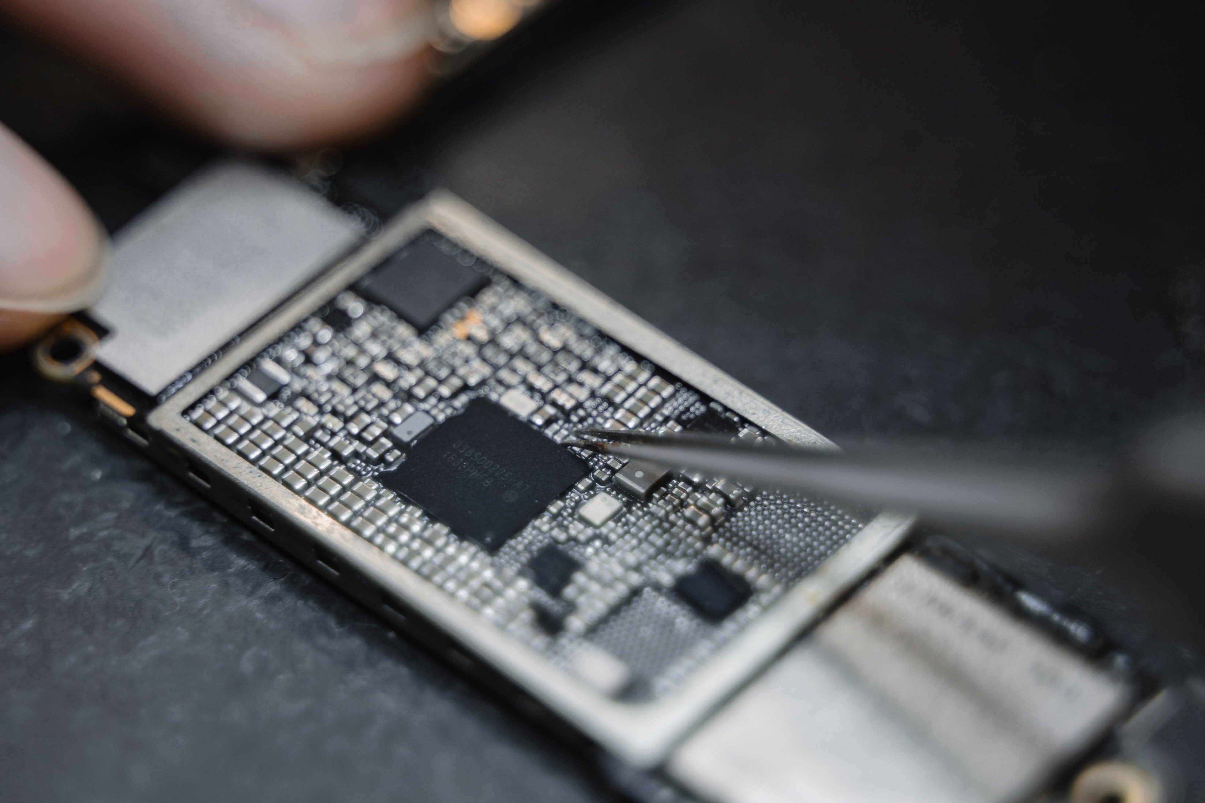
This advanced PCB has a higher wiring density that allows for a number of benefits for products. HDI PCBs have amplified performance levels while requiring similar or less space than other types of PCBs. Due to the smaller pads, designing HDI PCBs requires additional precision to conserve board space and match the fine pitch of circuitry found on the board. For applications that require high-layer count PCBs, HDI PCBs offer a solution that can reduce size and weight.
Benefits of HDI PCBs
By reducing the size and weight constraints, HDI PCBs also allow designers to position components on both sides of bare PCBs. By utilizing different via processes like via in pad or blind via technology, there are more ways to transmit faster signals and reduce crossing delays. As technology continues to advance, HDI PCBs will remain at the forefront of developing innovative products.
Contact Via Technology for HDI PCB Design
If you are interested in building products with HDI PCBs, contact Via Technology to learn more about how we can assist with your project. We offer an online quote form that can help you get started quickly with designing and launching your product.
