Multilayer PCBs

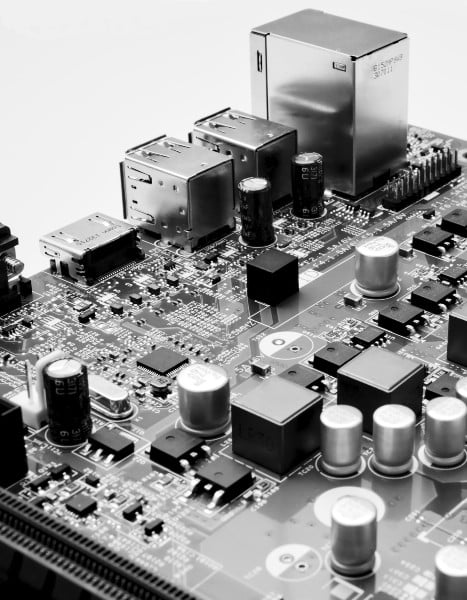
Multilayer PCBs are circuit boards with three or more layers of copper foil. Compared to single or double-sided PCBs, multilayer PCBs are smaller and have higher assembly densities. They also weigh less since there is less need for wiring harnesses.
Most sophisticated electronics use multilayer PCBs. Between four and eight layers are required for most applications, although twelve and even more layers are not unusual. Layers are usually found in even numbers, as odd numbers can cause circuit warping.
What Are Multilayer PCBs Used For?
Multilayer PCBs are particularly useful in the aerospace industry because they take up little room and are lightweight. They can also be found in cell phone repeaters, heart monitors, x-ray equipment, fiber optic receptors, atomic accelerators, nuclear detection systems and space probes.
Multilayer PCBs are also utilized in applications where crosstalk levels—electric or magnetic disturbance affecting the signal of an adjacent circuit—must be minimized.
How Complex Are Multilayer PCBs?
Multilayer PCBs are fabricated using layers of pre-peg and core materials which are laminated together under high pressure and temperature to remove any trapped air.
Because of the multiple layers, multilayer PCBs require more time at both the design and assembly phases. Multilayer PCBs are also more difficult to repair, should the need arise. Additionally, fabricating them is more expensive than alternatives, in part because of the cost of the machinery required to produce them.
Designing multilayer PCBs requires extensive pre-production design. Our skilled team members have the knowledge and experience to handle your multilayer PCB needs. To speak to them about your project, contact Via Technology today!
