Bare PCBs For Assembly

Bare PCBs For Assembly

Bare-PCBs-For-Assembly

Bare printed circuit boards (PCBs) are critical components for building custom circuitry in various electronic devices, including automobiles, smartphones, computers and more. Understanding the necessity of bare PCBs for testing and prototyping use cases can help you determine your needs for your next project.

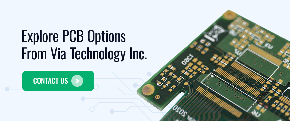
This guide will explain everything you need to know about applications for bare PCBs and how Via Technology Inc. can design purpose-built PCBs for your use case.

What Are the Components of Bare PCBs?

The bare PCBs are the fundamental electromechanical components that house the electronic parts and provide the electrical interconnects. They are made up of the following basic components:

  • Substrate material: This piece, typically constructed from fiberglass, provides a stable structure for the board’s electronic components.
  • Copper layers: Whether made from a solid copper coating or a piece of copper foil, this layer helps carry electrical signals to and from the board.
  • Solder mask: This polymer layer is essential for protecting the underlying components from damage due to exposure. 
  • Silkscreen layer: The silkscreen, sometimes called the nomenclature or legend, provides at-a-glance details on test points, switch settings and component references. It is typically located on the PCB’s component side.

Bare PCBs vs. Assembled PCBs

Bare circuit boards differ from assembled printed circuit boards (PCBAs). PCBs include only the fundamental four board components, and they serve as platforms for testing various board designs before adding more complexity through electronic components. 

Due to the absence of electronic components, PCBs are not functional — they cannot be used in fully operational electronic devices. In contrast, PCBAs are complete and can be effectively employed in electronic applications.

Types of Bare PCBs

There are five types of bare PC boards, each specialized for a different application:

  • Single-sided PCBs: A single-sided board has one layer of conductive copper, typically on the component side. This board type is best for simple applications due to its compact footprint and affordability.
  • Double-sided PCBs: Double-sided circuit boards have copper layers on both sides to accommodate more complex circuitry without requiring a significant size increase.
  • Multilayer PCBs: A multilayer PCB has three or more copper layers stacked on each other, allowing you to include highly complex circuitry while maintaining a compact board size.
  • Flexible PCBs: Also known as flexible electronics or flex circuits, flexible PCBs are designed to fit precisely in applications where space is limited.
  • Rigid-flex PCBs: Rigid-flex boards feature both a flexible and a rigid component. You can fold or bend the board to fit into different devices.

What Are Bare PC Boards Used For?

Bare PCBs are typically used to prototype and test new circuit designs. Because they lack electrical components, these boards make it easier for engineers to identify design flaws early in the process. 

This early identification can help your company save valuable time and money compared to testing fully assembled PCBs because it eliminates additional variables that can complicate the process.

Bare PC boards are also used for creating custom boards. They essentially serve as a blank canvas for engineers to design circuitry for applications with highly specific requirements.

Industry Applications for PCBs

Industry-Applications-for-PCBs.

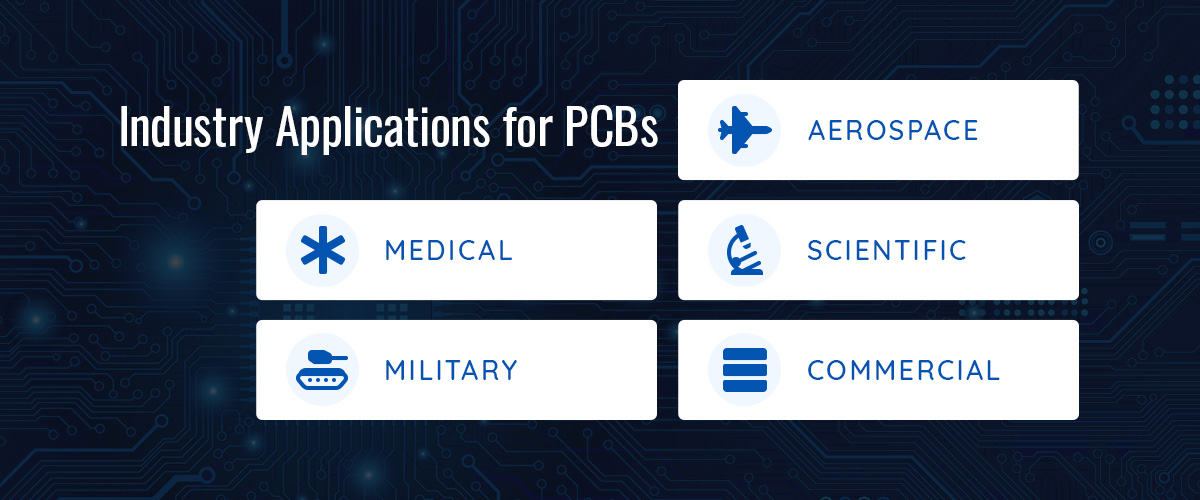
Regardless of the application, our professional team is capable of creating intricate and complex PCB prototypes of every scale. Our engineers have extensive experience designing boards for customers in various industries and sectors, including:

How Complex Are Bare PCBs?

Ultimately, a bare PCB’s complexity depends on its design. It is generally less complex than other types of PCBs, but it is important to remember these boards.

Several factors contribute to PCB complexity:

  • Layer count: PCBs become more complex the more conductive layers they have. For example, a multilayer PCB is significantly more complex in design than a single-layer board. 
  • Component density: Adding more electrical components in an area of the board increases its component density. Bare PCBs lack electronic components, making them less complex than other types of PCBs.
  • Trace width and spacing: Correct line spacing is critical for compliance with safety standards because improperly spaced traces can lead to arcing and malfunctions. While bare PCBs do not have electronic components soldered on to them, engineers must still take care to space the copper traces accordingly.
  • Via types and counts: The number, type and complexity of the vias used directly impact a board’s overall structure. 

The costs and difficulties of the bare PCB manufacturing process will vary depending on each board’s specific characteristics. More complex designs will result in longer, more costly manufacturing processes than simpler ones.

At Via Technology Inc., our bare PCBs include double-sided to multilayered configurations. We are able to support projects with a wide range of complexities through the capabilities of our bare PCBs.

Key Design Considerations for Bare PCBs

Some important factors to consider when designing a bare PCB include:

  • Electrical performance: Design factors like the board’s layout, the thickness of copper used, trace design and more are critical considerations for developing a board that optimizes electricity flow.
  • Thermal management: Heat sinks, cooling fans and other thermal management techniques are critical for controlling the board’s temperature. The method used on a board must fit into the available space of the application. 
  • Signal integrity: Boards must be able to maintain an electrical signal with minimal distortion, especially in high-speed applications. Via design, substrate selection and trace geometry are all important factors in creating a board that can conduct a strong and intact signal.
  • Board material: The substrate material used directly impacts board price, conductivity and durability, which can help you create a highly functional piece of technology with a long lifespan. 

The engineers at Via Technology, Inc. can design various types of bare PCBs to support many different use cases, including single-sided, double-sided, multilayer and more. From prototyping to circuit board testing, our bare PCBs are carefully designed to meet your needs.

Explore PCB Options From Via Technology Inc.

Sourced through our ISO 9001:2008 and ITAR-registered suppliers, our bare printed circuit boards are manufactured with exceptional quality. We thoroughly check our PCBs for consistency in accordance with industry standards. These PCBs form the backbone of assembly projects ranging from prototypes to completed products for commercial and consumer use.

Our certified suppliers enable us to quickly create fully turnkey solutions for your project. We completely cover PCB assembly with detailed testing and layout services. 

Contact Via Technology Inc. to get started with your PCB project today!

Explore-PCB-Options-From-Via-Technology-Inc.

Next ArticleRigid PCBs